


0571-26692003
No. 181 Geyazhuang, Xihu District,Hangzhou, Zhejiang, P.R. China

Driven by the new wave of information technologies powered by artificial intelligence and big data, high-speed transmission and low-power processing have become core demands for next-generation chip development. Photonic chips, which use photons instead of electrons to perform information processing and transmission, are widely regarded as a key pathway to overcoming the power consumption and speed bottlenecks of conventional microelectronic devices. Among them, phonon polaritons (PhPs) — quasiparticles formed by the strong coupling between light and lattice vibrations — can compress optical fields down to the nanoscale, providing a unique physical platform for building ultracompact, low-loss nanophotonic devices.
Recently, the research team led by Prof. Kehui Wu from Tsientang Institute for Advanced Study, in collaboration with Songshan Lake Materials Laboratory, has made important progress in the study of ternary molybdate polaritonic materials. Ternary metal molybdates with the general formula A₂(MoO₄)₃ (A = Al, Fe, Cr, etc.) host a wealth of exotic physical properties, including negative thermal expansion, ferroelastic phase transitions and elastic anisotropy. Strong optical phonon modes originating from MoO₄ tetrahedra inside the crystal lattice couple efficiently with mid-infrared photons, making this material family promising candidates for polaritonic applications.
Nevertheless, high-quality single-crystal growth of such molybdates has long remained a major bottleneck. Traditional solid-state synthesis requires heating above the sublimation temperature of MoO₃, which triggers molybdenum oxide volatilization and severe compositional imbalance, yielding only polycrystalline samples. Dense grain boundaries and structural defects in polycrystals mask intrinsic phonon responses and prevent direct nanoscale observation of phonon polariton propagation, greatly restricting their application in photonic devices.
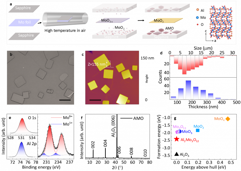
Figure 1. Interfacial epitaxial growth of Al₂(MoO₄)₃ single crystals.
To overcome these limitations, the team developed a low-cost, scalable interfacial epitaxy strategy relying on a confined-space design. High-purity molybdenum foil was sandwiched between two sapphire wafers to form a sandwich-confined structure. Upon annealing in air, the foil oxidized and sublimated to generate MoO₃ vapor precursors, which reacted with the sapphire surface to trigger interfacial nucleation followed by epitaxial growth of Al₂(MoO₄)₃ (AMO) nanoflakes.
This approach yielded nearly full coverage of AMO flakes across 2-inch c-plane sapphire wafers. The as-grown crystals featured atomically flat surfaces with an RMS roughness as low as 21 pm, confirming their outstanding single-crystalline quality. Furthermore, this growth method boasts great versatility and can be adapted to synthesize other ternary molybdates including Fe₂(MoO₄)₃ and Cr₂(MoO₄)₃.
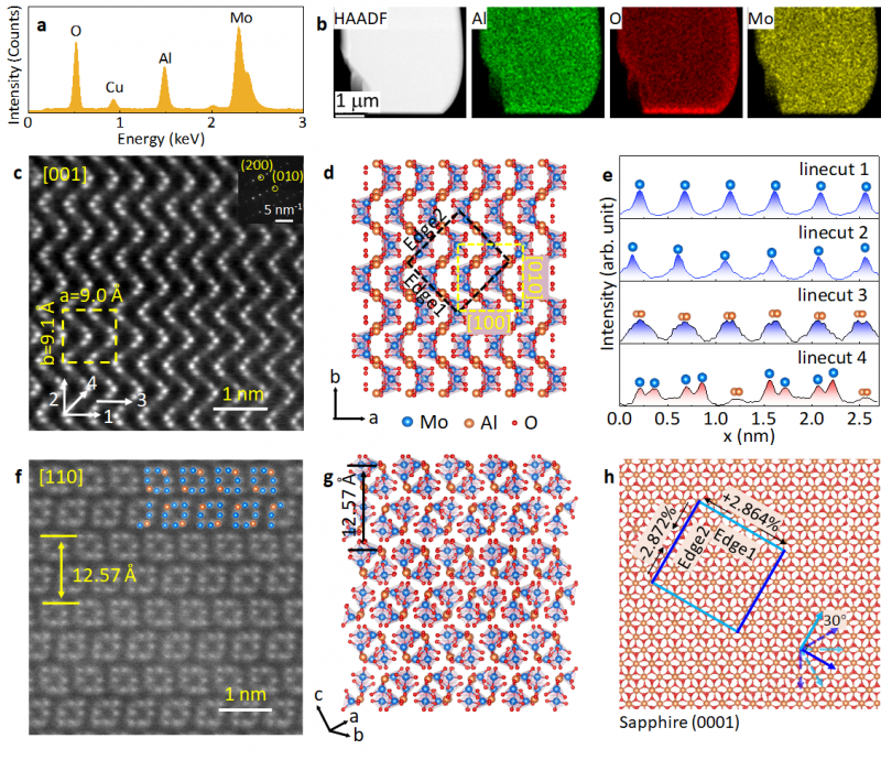
Figure 2. Atomic structural characterization of the AMO nanoflakes.
AMO forms a stable epitaxial interface with sapphire (0001) substrates and sustains controllable biaxial strain: +2.86% tensile strain along one orthogonal crystal edge and −2.87% compressive strain along the perpendicular direction.
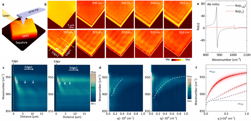
Figure 3. Anisotropic phonon-photon coupling in AMO flakes.
The biaxial strain breaks the in-plane lattice symmetry and induces strongly anisotropic propagation of phonon polaritons. Photo-induced force microscopy (PiFM) measurements show the polariton wavelength exhibits an anisotropy ratio of approximately 1.33 along the two orthogonal crystallographic axes. Density functional perturbation theory (DFPT) calculations on frequency-dependent dielectric tensors verify type-II hyperbolic polariton dispersion, which presents elliptic optical responses in-plane and hyperbolic responses out-of-plane. This novel material effectively remedies the spectral coverage blind spots of existing mainstream polariton materials such as hexagonal boron nitride and molybdenum trioxide.
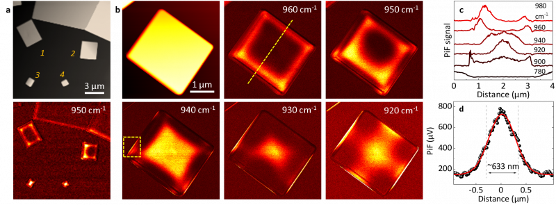
Figure 4. PhPs confinement in AMO crystal.
PiFM near-field imaging directly captures edge-launched phonon polaritons and their unique field evolution. As the excitation wavenumber decreases, polariton interference fringes launched from crystal edges gradually shrink into concentric rings and finally converge into a single, intense hot spot. At 930 cm⁻¹, free-space infrared light can be compressed by a factor of 17, demonstrating extraordinary optical field confinement capability for future super-resolution photonic components.
Combining controllable material synthesis, multi-dimensional microscopic characterization and first-principles theoretical simulation, this work establishes a universal fabrication framework for single-crystalline ternary molybdates. Benefiting from AMO’s strain-tunable anisotropic hyperbolic phonon polariton behavior, this new material platform opens up broad prospects for advanced photonic devices, including mid-infrared metalenses, on-chip integrated photonics and nanolasers.
This research received funding support from the National Key R&D Program of China, the National Natural Science Foundation of China, the Guangdong Basic and Applied Basic Research Foundation, Fundamental Research Funds for the Central Universities, and the Hangzhou Tsientang Education Foundation. The relevant work, titled Interfacial epitaxy of single-crystalline Al₂(MoO₄)₃ flakes for anisotropic phonon polaritons, was published online on June 25, 2026 in Nature Communications.
Corresponding authors
Kehui Wu ( khwu@tias.ac.cn )
Shaoxiang Sheng ( sxsheng@tias.ac.cn )
Chuangye Song ( cysong@tias.ac.cn )
Paper link: https://www.nature.com/articles/s41467-026-74681-x


